PixShift: A DIY Camera
Overview
PixShift is a project with the goal of creating a portable camera with a 8 by 8 pixel camera sensor that is mounted on a linear actuator so that images at a higher resolution (16 by 8 pixels) can be obtained. The camera sensor is created from scratch by laying out an 8 by 8 grid of phototransistors on a custom PCB. The PCB is then mounted on a linear actuator so that it may be shifted along the vertical axis. By displacing the PCB by a distance equivalent to half the distance between each row of sensors, PixShift can double its resolution along the vertical axis. The resulting camera is packaged into a portable, battery-powered form factor that saves all images take into a micro-SD card. When connected to a computer, a simple Python script can be used to display both 8x8 and 16x8 images through serial data.
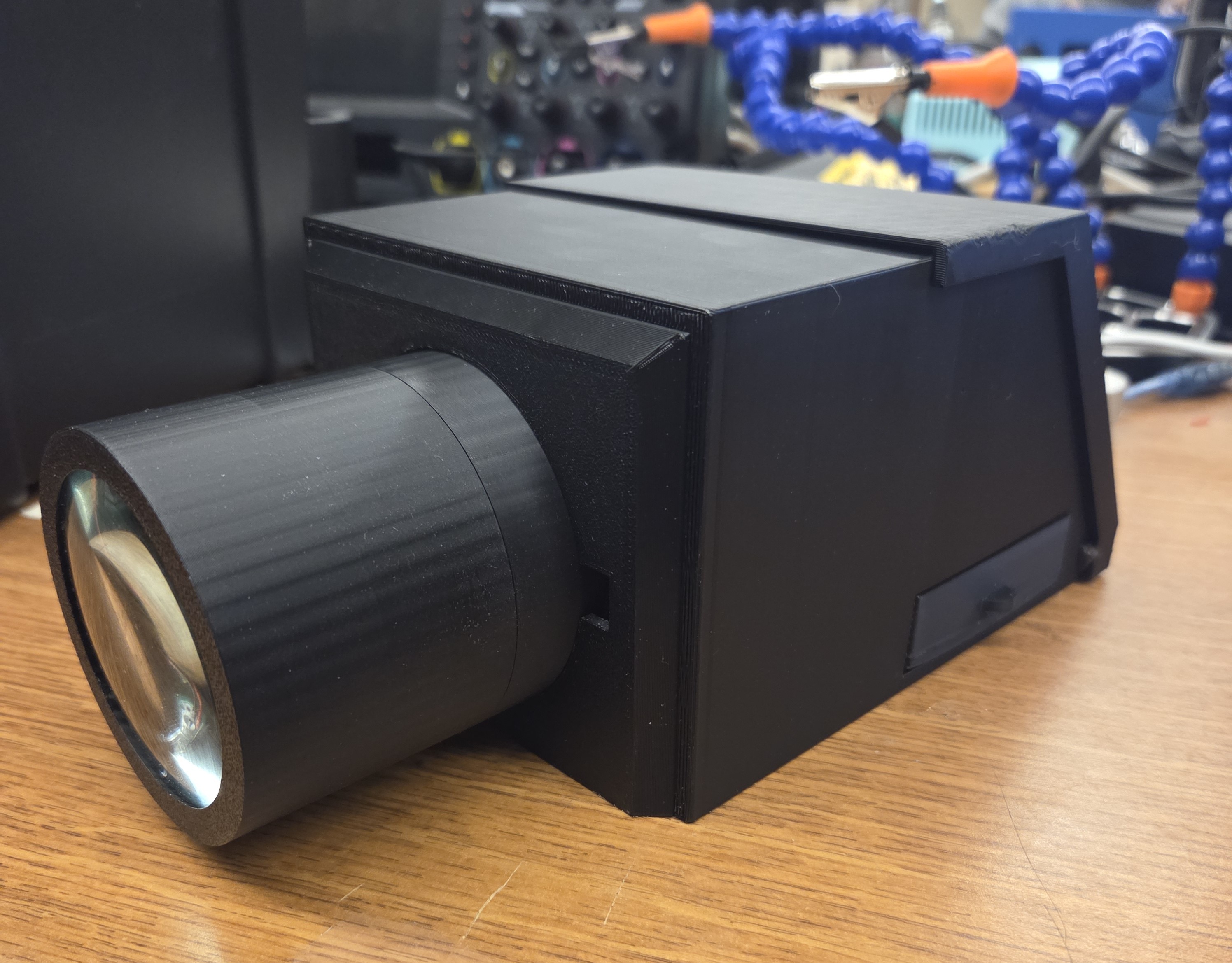
Figure 1. The finished camera.
Hardware
The primary hardware of this project is the custom PCB of phototransistors (Figure 2). It is a simple 2-layer board composed of 64 SMD ambient light sensors from Everlight and two 32-channel analog multiplexers (muxes) from Analog Devices. The left mux is responsible for feeding a fixed voltage to the collector of each phototransistor, which outputs a variable current based on the intensity of light (higher illuminance = higher current output), and the right mux receives that current and forwards it out of its drain terminal. Note that this board does not perform any computations.
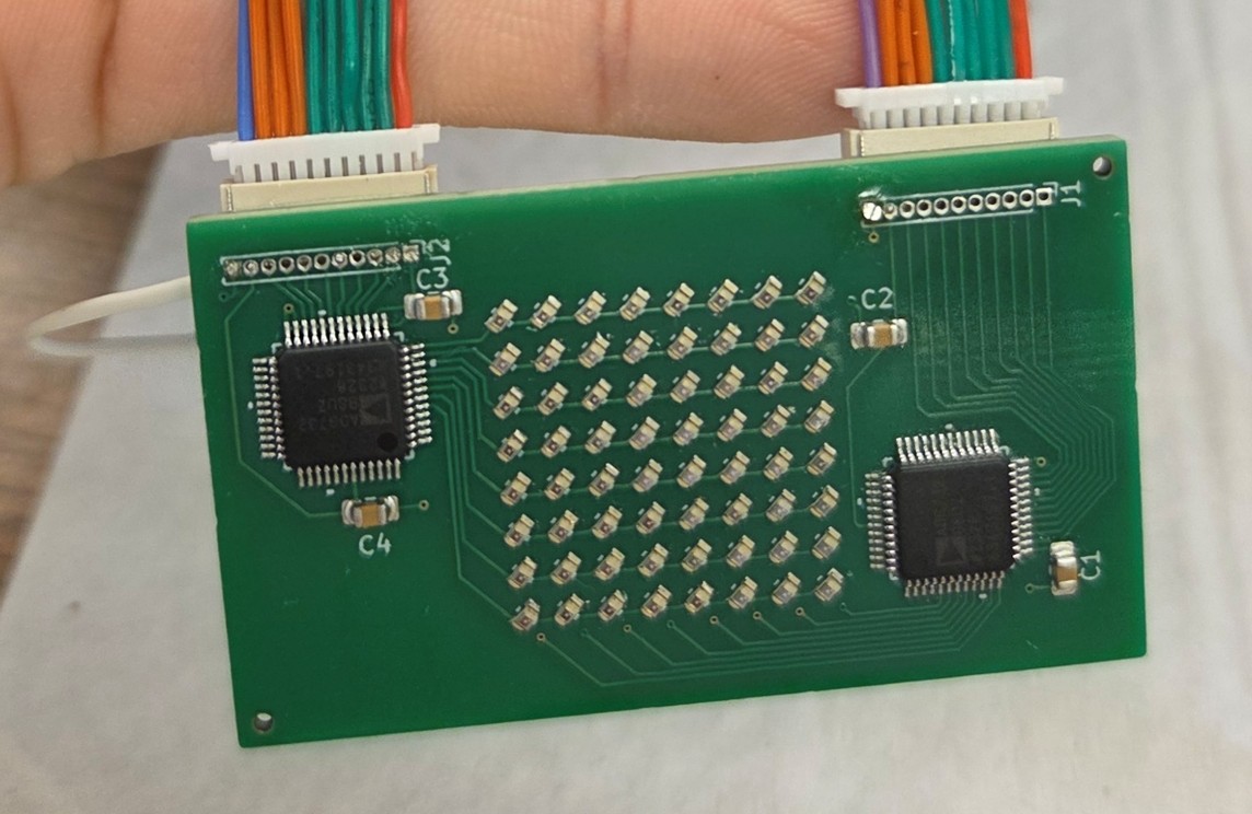
Figure 2. Camera sensor PCB board.
The next most important piece of hardware is the microcontroller. At the time of the proposal, an STM32 Nucleo-F411RE board was the initial choice. Later, it was switched to the Mega board in the Elegoo kits due to a greater familiarity with the development environment.
The linear actuator used is a DC 5V stepper motor with a linear rail (Figure 3), and it was sourced from Amazon. To control it, a mini-stepper motor control module (Figure 3) compatible with the stepper motor was purchased from Amazon as well. This controller is controlled with two buttons, but I wanted to control the motion of the actuator using digital pins on the Mega board, so I soldered two wires, one for each button, to write the active low signal to drive the actuator with the driver.
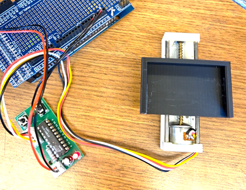
Figure 3. The linear actuator's stepper motor is being driven by the driver module but controlled by the digital pins on the Mega board.
The last main piece is a micro-SD card module, which I connected to the corresponding SPI pins on the Mega board to save images on an attached micro-SD card.
Libraries
Few libraries were used for this project. The only libraries used were the SPI and SD library, for the sole purpose of writing the buffered images into a persistent storage for later review. The remainder of the codebase does not depend on any library.
Designed Parts
The camera sensor is a custom PCB designed by me using Kicad. The final board was fabricated and assembled by JLCPCB. Due to an error on my design, I had to re-evaluate how to connect the pins of the PCB to my microcontroller board. After initial struggles with attempting to solder 28-gauge wires through the small pin holes on the PCB, I arrived at a much better solution, which was to use JST connectors (as shown in Figure 2).
The other main parts designed solely by me were the parts that make up the camera body. I have decided to 3D print the entire camera body using black PLA filament to reduce the amount of reflections within the camera. This was a great challenge for me since I had little CAD experience and virtually no 3D printing experience prior to this project. I also made it quite difficult on myself because I designed all the pieces of the camera body with the goal of not using any screws or glue; this meant that I had to learn how to CAD and print threads correctly. There were many failed attempts (Figure 4.), most of which were struggles with trying to find the correct offset for the threads so that two pieces can screw onto one another. I was eventually able to succeed, and this struggle also allowed me to become significantly better at CAD than before.
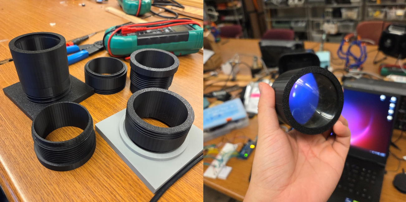
Figure 4. (Left) Failed attempts at 3D printing the pipe for the lens. (Right) A successful attempt at 3D printing a screw on lens cap.
Struggling with the lens cap allowed me to get more comfortable with CADing, so I decided to explore a different way of attaching the lens to the camera body. I ultimately decided on a twist-on locking mechanism where I first put the lens into a matching slot on the camera body, then twist to lock it in place (Figure 5).
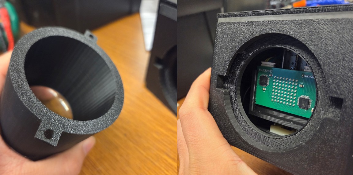
Figure 5. (Left) The camera lens has extrusions to lock it onto the camera body. (Right) The camera body has a matching slot as well as enough clearance to turn the lens and lock it in place.
Another minor piece that I designed other than the camera body is this little protoboard of three buttons that triggers an active-high signal when pressed. It serves as the primary source of input for the camera.
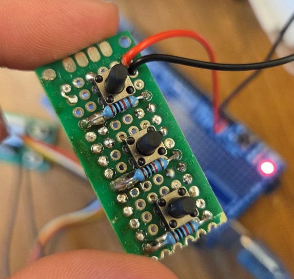
Figure 6. Three active high-buttons.
Iterative Testing
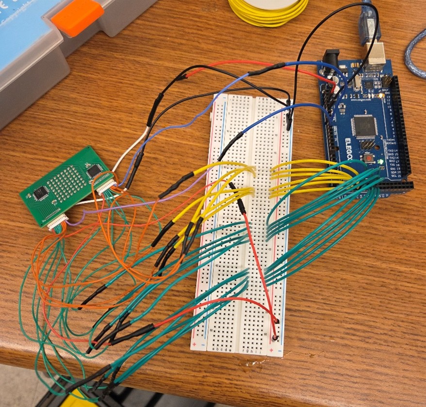
Figure 7. Initial testbench for the camera sensor.
Upon receiving the assembled PCB for the camera sensor, I went to test it with the initial testbench shown above (Figure 7) to see if it was working as expected. This initial made me realize a couple mistakes I made when designing the camera sensor PCB. First, the phototransistors I was using are light to current devices, and I needed to convert that current output into a voltage. Furthermore, it also made me realize that the rise and fall times of the phototransistors are quite long, and if I did not give them enough time to settle, I would get some highly variable and confusing results.
In the second testbench (Figure 8), I connected the output pin to a 2K load resistor to convert the current output from the camera sensor into a voltage reading. This new testbench made me realize the importance of the load resistor on the behavior of the phototransistor, and after consulting the datasheets and running several experiments, I have decided to use a 47K load resistor. I also realized that each sensor has some slight variations; for example, even when stimulated by the same strength of light, two sensors might read different high values. To mitigate such variations, I decided to implement a calibration procedure that uses a flat bright frame and dark frame to compute the gain of each pixel, which is then used to correct the readings of each pixel through the formula: corrected_reading = (raw_reading - dark_reading) * gain. The three buttons are created to make this calibration process easier to repeat.
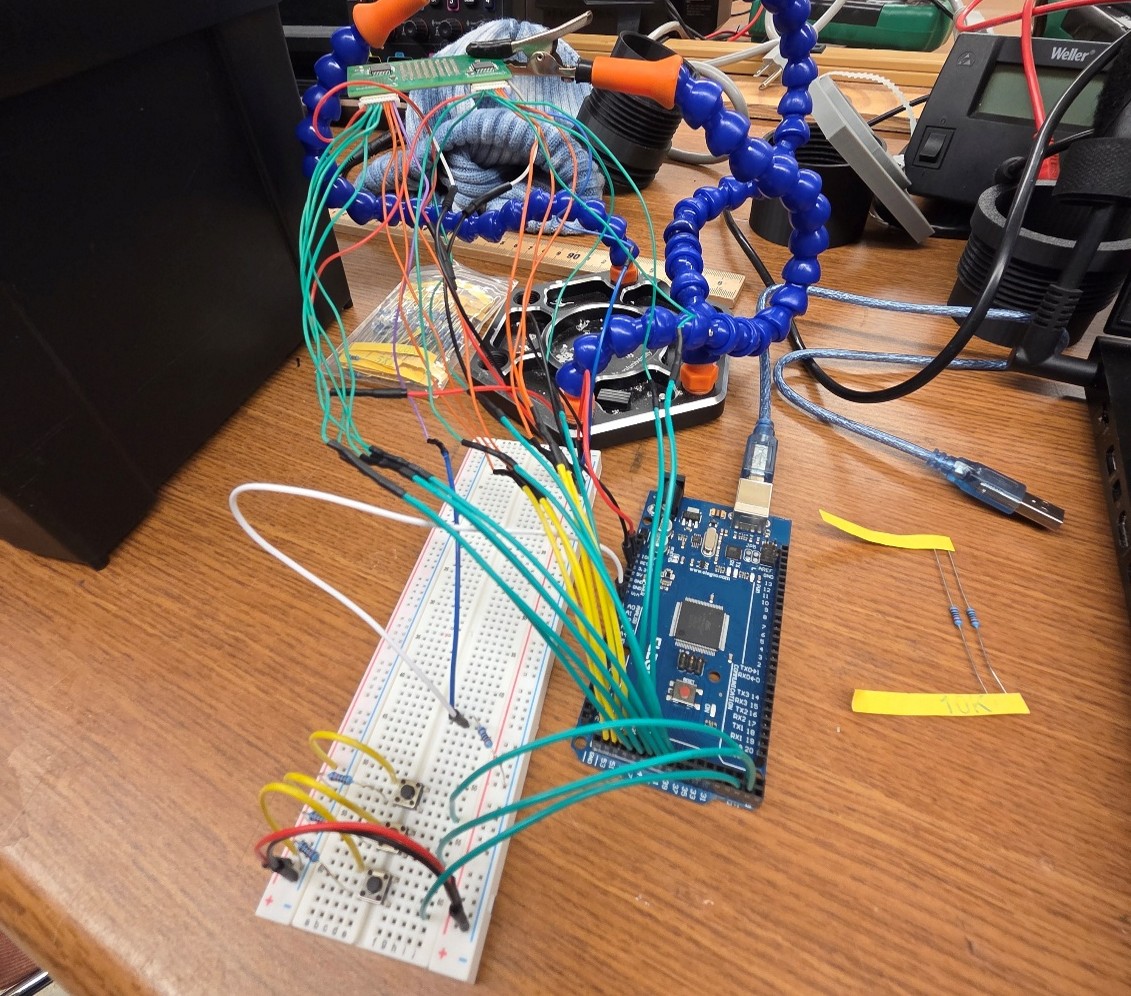
Figure 8. Improved testbench for the camera sensor PCB.
Once I am confident that the sensor and my corresponding program work, I begin the process of shifting what I have from the breadboard onto the protoboard compatible with the Mega board and trying to fit everything inside the camera. The result is shown below (Figure 9). In the meantime, I also soldered on the stepper motor driver and the micro-SD card module. After soldering. however, the sensor PCB began to produce erratic and unexpected outputs; I suspected that it was due to the insecure connection between the 3.3V pin and the voltage in pins of the sensor along with the insecure connection of the ground pins. After failed attempts to fix the problem, I decided to cut all the wires soldered onto the center of the protoboard and replace it with a breadboard (Figure 9). This solved the problem I was having. This also made it much easier for me to run some other minor experiments, such as using a potentiometer to control the voltage going into the sensor, as well as adding an active beeper to play a specific tone for every distinct action.
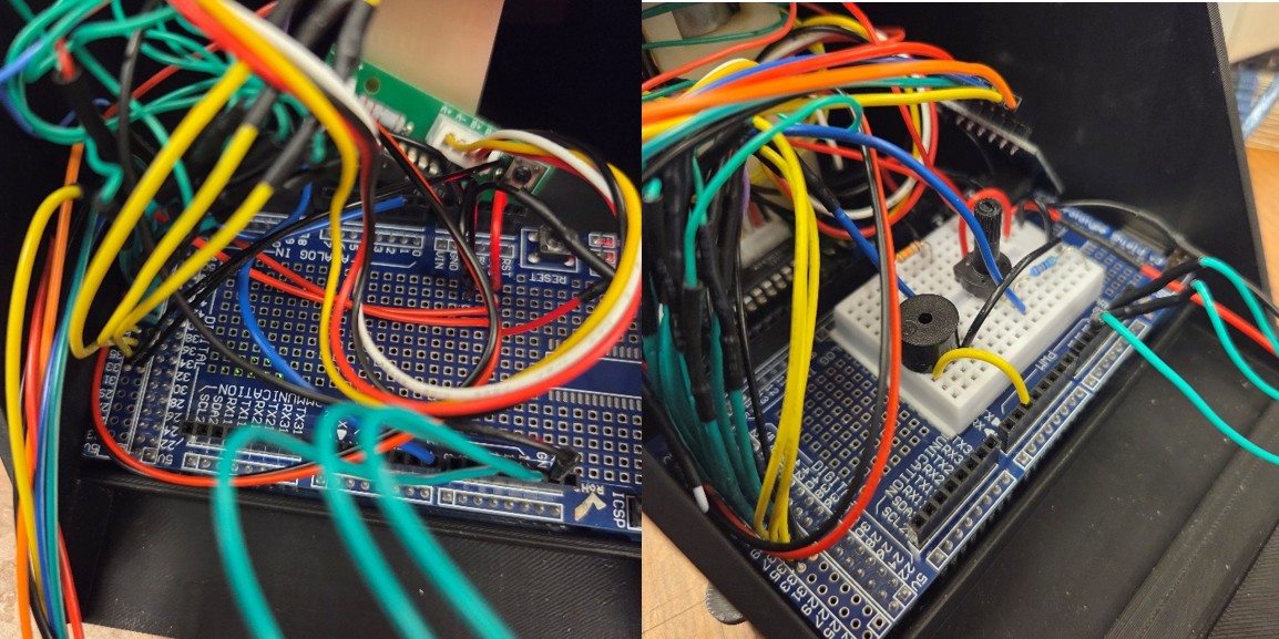
Figure 9. (Left) All components soldered onto the protoboard on the Mega board, but it did not work. (Right) Replaced all connections in the center with a breadboard.
Finally, with most of the camera complete, the rest of the testing is done through a Python script displaying the 8x8 and 16x8 images from the camera so that I can visually analyze the results. Figure 10 shows an example of the 8x8 image as I moved a cotton ball with a tweezer to obstruct light from certain parts of the sensor.

Figure 10. The reading from the sensor array with a cotton ball obstructing light near the center left.
Skills I had to Learn
- I learned Kicad in two days using a video series provided by the Hive Makerspace, design the sensor array circuit in a day, then spent another day laying out the PCB and figuring out how to use fabrication services like PCBWay and JLCPCB.
- I have never personally 3D printed before, and it has been so long since I last CADed that my old OnShape account expired years ago due to inactivity, so I am essentially a novice in both CADing and 3D printing. I viewed this project as an opportunity for me to explore interesting things that you can make with a 3D printer. One such interesting thing is how to connect pieces without the use of glue or screws.
Results
The following are some of the results!
Video 1. Example of 8x8 pixel image reading as a flashlight is moved across the camera's FOV.
Video 2. Example of 16x8 pixel image reading as a flashlight is moved across the camera's FOV.